基本信息
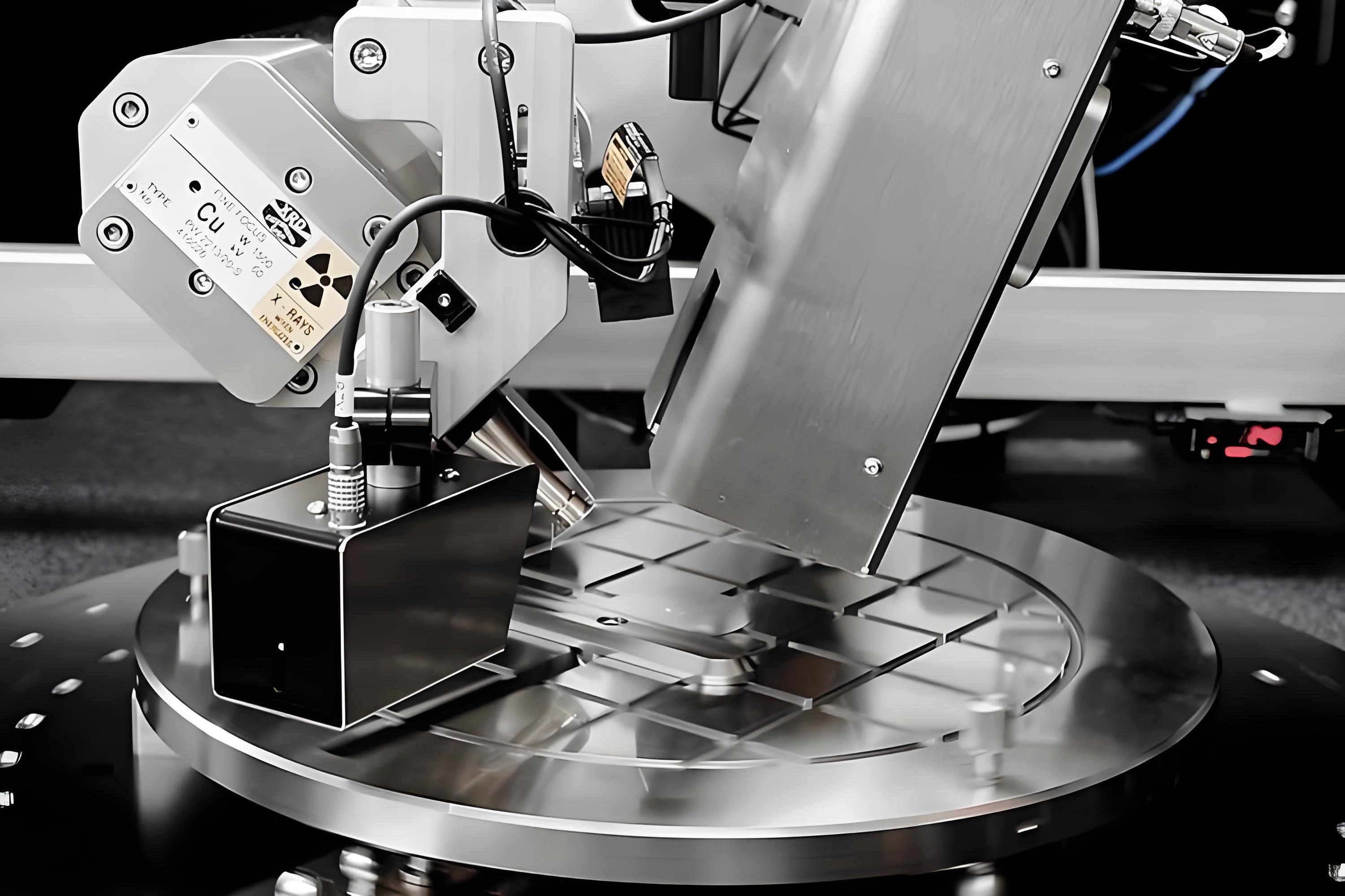
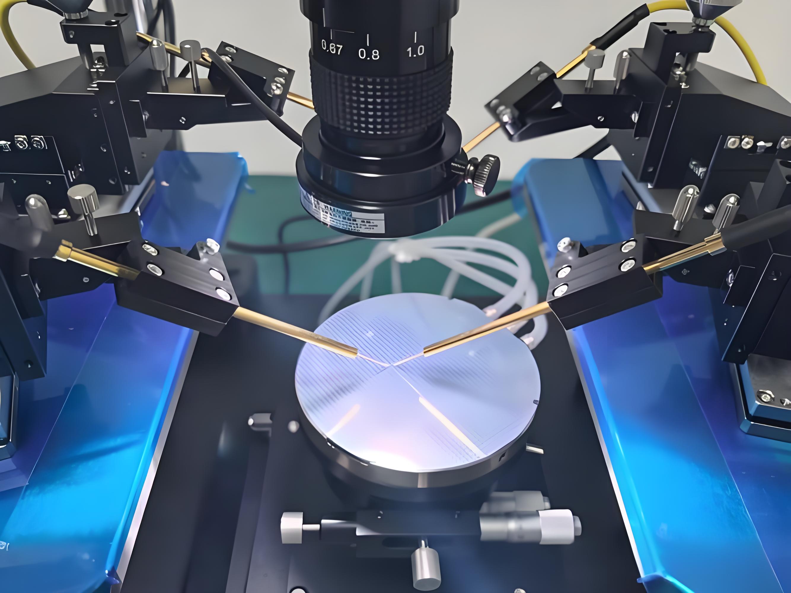
This automated wafer level profile metrology system is a professional high-precision measuring equipment for the semiconductor manufacturing industry. It can realize fully automatic detection of the contour, flatness and step height of semiconductor wafers, solving the pain point of low efficiency and high error rate of manual detection in the semiconductor production line. It is suitable for wafer manufacturing, microelectronic component production and other scenarios, helping enterprises improve the detection efficiency of semiconductor products and ensure the quality of finished products.


 发布询价
发布询价


 聊天
聊天


 所有分类
所有分类